W1TAG / WD2XES / WE2XGR/3
John K. Andrews
Holden, MA FN42ch
[ w1tag@charter.net ]
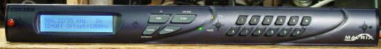
WE2XGR/3 SSB Exciter
What it Does:
While it is unlikely that SSB voice operation is suited to the narrow frequency allocation at 505-510 kHz, an SSB
exciter does allow use of a host of soundcard-based digital modes. PSK31 is the most familiar of these, but there are
plenty of others! The exciter pictured above was built into a discarded prototype chassis for a product manufactured by
my employer, Comrex Corporation. Nice of them to pay for the industrial engineering.
Frequency Control:
A 10 MHz output from an HP Z3801 GPS receiver is used for the time base of an Analog Devices AD9851 DDS chip. That chip
outputs the range of frequencies from 2020 to 2060 kHz, four times the nominal carrier frequency. The output of the DDS
is a square wave in this application. The DDS is run by
an Atmel 89C51-AC2 microcontroller, which also connects to the front panel display and keypad. The micro is programmed
in assembly language, using many routines from earlier LF exciters, plus some new ones. There is a menu system which
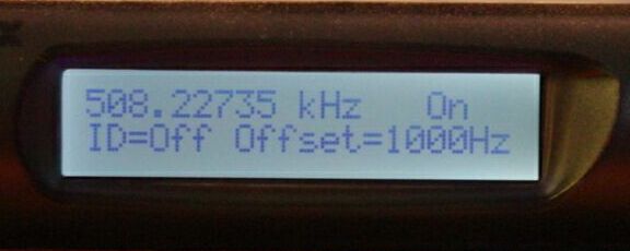
allows selection of frequency, offset corresponding to the input audio frequency, and a 30 minute ID. The display gives a nice
summary of the current operating status:
Phasing Exciter:
Audio from a sound card is fed through an input level control and peak-reading LED audio level meter. I took advantage of
an old 90 degree audio phase shift board from work. This was cut from a larger bare board using a bandsaw. You can't do this
with multilayer boards! This is a ten section all-pass filter, redesigned specifically for the 100 to 3500 Hz range. Carefully
selected parts were used to match the actual 3 dB breakpoint frequencies with the theoretical values. This was helped by the
availability of a Philips digital RLC bridge. A phase plot shows that
the extra work was justified. A pair of balanced line buffer chips provide outputs at 0, 90, 180 and 270 degrees, which are fed
to an analog multiplexer chip. The 2 MHz square wave from the DDS feeds a Johnson counter, which is decoded by the multiplexer.
An earlier design with single-ended switch had some unwanted spurs. In this exciter, a dual multiplexer provides a balanced circuit
which cancels some of the spurs, leaving a very clean output. The LSB is suppressed by 55 dB, and the carrier by 48 dB. I'm planning
to do further work to improve the carrier suppression.
Output Stages:
A dual op-amp sums the outputs of the dual multiplexer chip, and feeds a 5-element low pass filter. The output is routed through a
front-panel level pot, and then to an output buffer amplifier capable of providing 100 mw into 50 ohms. The output is quite clean, with
the second harmonic down about 50 dB. The output is a true 50 ohms, which allows use of a calibrated step attenuator between the exciter
and the power amplifier, which has a 50 ohm input impedance.
The Insides:
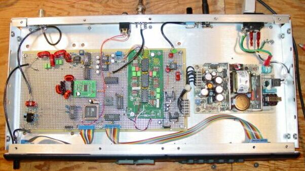
The commercially-made switching power supply (it came with the chassis) is on the right, and produces +5, +15 and -15 VDC. There are
two daughter boards on the large perfboard. The one on the right (with the 3 chips) is the audio phasing network. The small green
board in the center has the DDS chip. The microcontroller circuitry is in the front center area, and the balanced modulator is at
the back. The output stage is on the left.
Back to Home